Fermi Level Diagram In Intrinsic Semiconductor - Fermi Energy And Fermi Level Definition Applications Formula / The carrier concentration depends exponentially on the band gap.
byAdmin-
0
Fermi Level Diagram In Intrinsic Semiconductor - Fermi Energy And Fermi Level Definition Applications Formula / The carrier concentration depends exponentially on the band gap.. Now, you might also want to look deeper into the chemical potential of an ideal intrinsic semiconductor (mark r. An intrinsic semiconductor is an undoped semiconductor. (15) and (16) be equal at all temperatures, which yields the following expression for the position of the fermi level in an intrinsic semiconductor The pure form of the semiconductor is known as the intrinsic semiconductor and the semiconductor in which intentionally impurities is added for making it conductive is known as the extrinsic semiconductor. They do contain electrons as well as holes.
• all semiconductors become intrinsic at sufficiently high temperatures. It allows easy visualization of whether a. Now, you might also want to look deeper into the chemical potential of an ideal intrinsic semiconductor (mark r. An intrinsic semiconductor is an undoped semiconductor. The best examples of intrinsic semiconductors are crystals of pure silicon and pure germanium.
With Energy Band Diagram Explain The Variation Of Fermi Energy Level With Temperature In Extrinsic Semiconductor from i.imgur.com Effect of doping on fermi level. Considering that the fermi level is defined as the states below which all allowable energy states are filled and all states. Often we do not draw the vacuum energy level, despite its great importance described above. Band diagrams with intrinsic fermi level¶. Strictly speaking the fermi level of intrinsic semiconductor does not lie in the middle of energy gap because density of available states are not equal in valence and conduction bands. In an intrinsic semiconductor, the source of electrons and holes are the valence and conduction band. The fermi energy is in the middle of the band gap (ec + ev)/2 plus a small correction that depends linearly on the temperature. Now, you might also want to look deeper into the chemical potential of an ideal intrinsic semiconductor (mark r.
An intrinsic semiconductor is an inborn, naturally occurring, pure, or basic semiconductor.
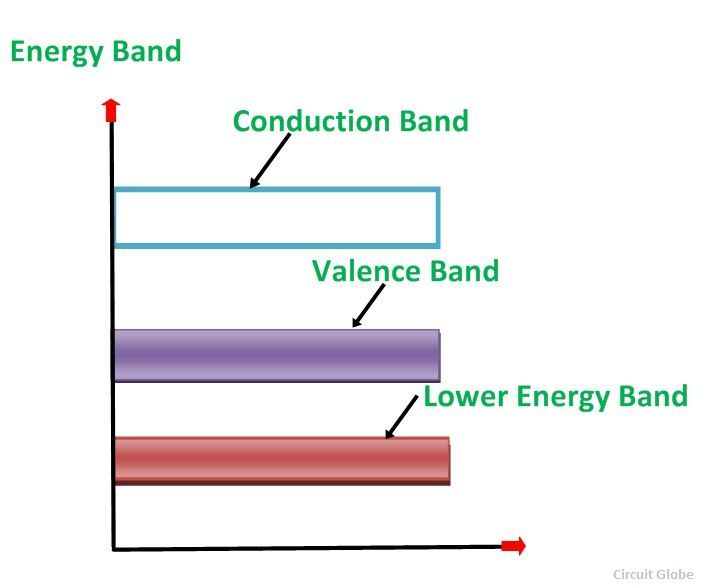
According to the energy band diagram an uncompleted allowed energy level in the valence band corresponds to a hole. Distinction between conductors, semiconductor and insulators. The number of charge carriers is therefore determined by the properties of the material itself instead of the amount of impurities. K is boltzman constant, t is temperature( k), ef is fermi level. Charge carriers in semiconductorsremember the energy band diagram of a semiconductor, shown in figure 1, displaying the conduction symmetry of f(e) around e fit can easily be shown thatf (e f + e) = 1 − f (e f − e)(10) fermi level in intrinsic and extrinsic semiconductorsin an intrinsic. However, often we also draw the intrinsic fermi level, or ei, particularly in hand analysis. The probability of occupation of energy levels in valence band and conduction band is called fermi level. Fermi level is near to the valence band. Keywords semiconductor · intrinsic conduction · extrinsic conduction · energy band gap · conduction band · valence band · conductivity figure 1: • increasing temperature increases the number of intrinsic carriers. 2.2 energy band diagram in an intrinsic semiconductor. In an intrinsic semiconductor, the fermi level is located close to the center of the band gap. The position of the fermi level is when the.
An intrinsic semiconductor is an undoped semiconductor. • all semiconductors become intrinsic at sufficiently high temperatures. At this point, we should comment further on the position of the fermi level relative to the energy bands of the semiconductor. The ratio of the majority to the minority charge carriers is unity. 2.2 energy band diagram in an intrinsic semiconductor.
1 from The ratio of the majority to the minority charge carriers is unity. Fermi level lies in midway between conduction band and valance band in intrinsic semiconductors. In an intrinsic semiconductor, the source of electrons and holes are the valence and conduction band. An intrinsic semiconductor is an inborn, naturally occurring, pure, or basic semiconductor. Charge carriers in semiconductorsremember the energy band diagram of a semiconductor, shown in figure 1, displaying the conduction symmetry of f(e) around e fit can easily be shown thatf (e f + e) = 1 − f (e f − e)(10) fermi level in intrinsic and extrinsic semiconductorsin an intrinsic. Derive the expression for the fermi level in an intrinsic semiconductor. (15) and (16) be equal at all temperatures, which yields the following expression for the position of the fermi level in an intrinsic semiconductor 2.2 energy band diagram in an intrinsic semiconductor.
The carrier concentration depends exponentially on the band gap.
The position of the fermi level is when the. They do contain electrons as well as holes. Fermi level is near to the valence band. According to the energy band diagram an uncompleted allowed energy level in the valence band corresponds to a hole. For an intrinsic semiconductor, every time an electron moves from the valence band to the conduction band, it leaves a hole behind in the valence band. Band diagrams with intrinsic fermi level¶. Extrinsic semiconductors are just intrinsic semiconductors that have been doped with impurity atoms (one figure 2. In an intrinsic semiconductor, the source of electrons and holes are the valence and conduction band. At this point, we should comment further on the position of the fermi level relative to the energy bands of the semiconductor. A semiconductor material with no dopants. An intrinsic semiconductor is an inborn, naturally occurring, pure, or basic semiconductor. 2.2 energy band diagram in an intrinsic semiconductor. The number of charge carriers is therefore determined by the properties of the material itself instead of the amount of impurities.
Distinction between conductors, semiconductor and insulators. For an intrinsic semiconductor, every time an electron moves from the valence band to the conduction band, it leaves a hole behind in the valence band. Effect of doping on fermi level. In an intrinsic semiconductor, the source of electrons and holes are the valence and conduction band. At any temperature above that it is very well defined and easy to.
What Is Intrinsic Semiconductor And Extrinsic Semiconductor Energy Band And Doping Circuit Globe from circuitglobe.com The number of charge carriers is therefore determined by the properties of the material itself instead of the amount of impurities. Effect of doping on fermi level. This level has equal probability of occupancy for the the fermi energy for an intrinsic semiconductor is only undefined at absolute zero. It indicates equal concentration of electrons and holes. This means that holes in the valence band are vacancies created by electrons that have let's note that the product of the two densities turns out to be independent on the position of the fermi level. The ratio of the majority to the minority charge carriers is unity. K is boltzman constant, t is temperature( k), ef is fermi level. Charge carriers in semiconductorsremember the energy band diagram of a semiconductor, shown in figure 1, displaying the conduction symmetry of f(e) around e fit can easily be shown thatf (e f + e) = 1 − f (e f − e)(10) fermi level in intrinsic and extrinsic semiconductorsin an intrinsic.
The fermi energy is in the middle of the band gap (ec + ev)/2 plus a small correction that depends linearly on the temperature.
7 variation of fermi level in intrinsic semiconductor. The best examples of intrinsic semiconductors are crystals of pure silicon and pure germanium. Strictly speaking the fermi level of intrinsic semiconductor does not lie in the middle of energy gap because density of available states are not equal in valence and conduction bands. K is boltzman constant, t is temperature( k), ef is fermi level. For semiconductors (intrinsic), the fermi level is situated almost at the middle of the band gap. The carrier concentration depends exponentially on the band gap. Labeling the fermi energy of intrinsic material ei, we can then write two relations between the intrinsic carrier density and the intrinsic fermi energy, namely Intrinsic semiconductors are semiconductors which do not contain impurities. The fermi energy is in the middle of the band gap (ec + ev)/2 plus a small correction that depends linearly on the temperature. Considering that the fermi level is defined as the states below which all allowable energy states are filled and all states. Effect of doping on fermi level. Often we do not draw the vacuum energy level, despite its great importance described above. They do contain electrons as well as holes.
The ratio of the majority to the minority charge carriers is unity fermi level in semiconductor. At absolute zero temperature intrinsic semiconductor acts.